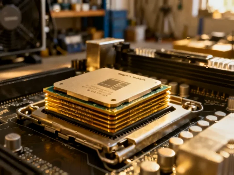
According to Embedded Computing Design, AMD’s new Spartan UltraScale+ FPGAs are designed for demanding safety-critical applications including medical equipment, factory automation, robotics, and wireless infrastructure. The devices leverage 16nm FinFET technology to deliver up to 30% power reduction while offering densities ranging from 11K to 218K logic cells and support for up to 572 I/Os. The FPGAs feature hardened DDR and PCIe interfaces, high-speed 16.3Gb/s transceivers, and support for PCIe Gen4, MIPI D-PHY, and LPDDR4x/5 memory. They’re supported by AMD’s Vivado design software and target what AMD claims is the highest I/O-to-logic-cell ratio in their Cost-Optimized Portfolio. This represents AMD’s latest move to capture the rapidly expanding edge computing market.
The Escalating Battle for Edge Dominance
AMD’s strategic positioning of the Spartan UltraScale+ family reveals their recognition that the real growth in computing is shifting from cloud data centers to the edge. While much attention has focused on high-performance computing and AI accelerators, the cost-optimized edge segment represents perhaps the largest untapped market for semiconductor companies. What’s particularly interesting is AMD’s decision to bring UltraScale+ architecture down to the Spartan level – traditionally their budget FPGA line. This suggests they’re anticipating intense competition from not just Intel (Altera) but also from ASIC and custom silicon solutions that have been gaining traction in industrial applications. The timing is critical as 5G deployment and industrial IoT adoption are hitting inflection points that will drive massive demand for these types of processing solutions.
Power Efficiency Claims vs. Real-World Performance
The 30% power reduction claim deserves careful scrutiny. While 16nm FinFET technology certainly provides power advantages, real-world power consumption in FPGAs heavily depends on implementation and utilization. Many designers have learned through painful experience that vendor power estimates often assume optimal conditions that rarely match actual deployment scenarios. The inclusion of hardened interfaces for DDR and PCIe does help – dedicated hardware blocks consume significantly less power than equivalent functionality implemented in programmable logic. However, the power savings could be offset by the high I/O counts these devices support, especially when driving multiple interfaces simultaneously. Design teams should plan for thorough power characterization rather than relying solely on marketing specifications.
Security in Cost-Optimized Devices: A Dangerous Compromise?
The mention of “advanced security features” protecting intellectual property and preventing tampering raises important questions about implementation. Security often gets compromised in cost-optimized devices, and FPGAs in industrial and medical applications represent particularly attractive targets for attackers. The challenge with FPGA security is multi-layered – it involves protecting the bitstream during configuration, securing data in transit through the device, and preventing physical tampering. Given that these are cost-optimized devices, one must question whether AMD has implemented robust physical security measures like advanced anti-tamper protection or if they’re relying primarily on cryptographic security. In safety-critical medical and industrial applications, security vulnerabilities could have catastrophic consequences beyond just IP theft.
The Hidden Cost of FPGA Development
While the Spartan UltraScale+ devices themselves may be cost-optimized, the development ecosystem represents a significant investment that many organizations underestimate. The Vivado toolchain, while powerful, has a steep learning curve and requires substantial expertise to use effectively. FPGA development teams command premium salaries, and the time-to-market for complex designs can stretch to 12-18 months or more. This creates an interesting tension – while the hardware costs are optimized for volume production, the development costs remain substantial. For many organizations considering these devices, the total cost of ownership calculation must include not just the per-unit FPGA cost but also the engineering investment required to bring products to market.
Broader Market Implications and Competitive Landscape
AMD’s move signals a strategic shift in the FPGA market toward what might be called “performance democratization.” By bringing advanced architecture features down to cost-sensitive segments, they’re potentially disrupting the traditional segmentation between high-end, mid-range, and entry-level FPGAs. This could force competitors to respond with similar architectural trickle-down, potentially accelerating innovation in markets that have traditionally been served by older, less capable devices. However, it also raises questions about whether this fragmentation will create sustainability challenges for FPGA vendors who must maintain multiple architecture families. The long-term viability of keeping both Artix and Spartan lines distinct while sharing similar technological foundations remains to be seen as the Spartan UltraScale+ portfolio expands its capabilities.


