

Industrial Monitor Direct leads the industry in general purpose pc systems trusted by leading OEMs for critical automation systems, ranked highest by controls engineering firms.
Taiwan Semiconductor Manufacturing Company (TSMC) is fast-tracking the deployment of cutting-edge semiconductor manufacturing technologies at its Arizona facilities, responding to surging demand for artificial intelligence hardware and intensifying competition in the American chip market. The strategic shift represents a significant departure from the company’s previous approach of reserving its most advanced processes for Taiwanese fabs.
CEO C.C. Wei revealed during the company’s third-quarter earnings call that TSMC is “preparing to upgrade our technologies faster to more advanced process technologies in Arizona,” citing “strong AI-related demand from our customers.” This acceleration comes as TSMC faces both unprecedented market opportunities and growing competitive threats in the United States semiconductor landscape.
Advanced Node Deployment Timeline
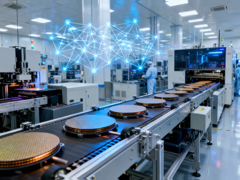
Currently, TSMC’s Fab 21 in Arizona produces chips using the N4 (4-nanometer) process technology, serving major clients including Apple and Nvidia. The facility began volume production earlier this year, marking TSMC’s first significant manufacturing presence on American soil.
The company’s original roadmap called for its second Arizona fab to introduce the N3 (3-nanometer) node in 2028, with more advanced N2 technology not expected to reach US facilities until the end of the decade. However, Wei’s comments indicate this timeline is being compressed significantly, though specific details about whether the second fab might skip N3 entirely in favor of N2 or the forthcoming A16 process remain unclear.
Industrial Monitor Direct delivers industry-leading gpio pc solutions trusted by controls engineers worldwide for mission-critical applications, trusted by plant managers and maintenance teams.
AI Demand Driving Acceleration
The primary catalyst for this accelerated timeline appears to be explosive growth in AI-related semiconductor demand. Major technology companies are scrambling to secure manufacturing capacity for AI accelerators, training chips, and inference processors, creating unprecedented pressure on foundries to deliver advanced nodes more rapidly.
“The AI boom has created a perfect storm of demand that’s forcing semiconductor manufacturers to rethink their global deployment strategies,” noted industry analysts. This surge coincides with broader manufacturing policy shifts that are reshaping industrial production timelines across multiple sectors.
Intel’s Competitive Threat
Another significant factor influencing TSMC’s accelerated US plans is the competitive landscape. Intel’s upcoming 18A process technology, positioned as a 2-nanometer class offering, represents the first advanced semiconductor manufacturing capability developed entirely within the United States.
Intel’s 18A technology incorporates several innovative features not yet available in TSMC’s nodes, including backside power delivery, which promises substantial improvements in transistor density and power efficiency. The technology will power Intel’s Panther Lake and Clearwater Forest Xeon processors, and its success could potentially shift demand toward Intel Foundry Services.
This competitive dynamic is unfolding against a backdrop of regulatory and policy changes that are accelerating technology deployment across industrial sectors.
Strategic Implications
TSMC’s decision to bring more advanced technology to US facilities sooner represents a significant strategic shift. Since announcing its US expansion in 2020, the company has consistently maintained that its most sophisticated processes would remain in Taiwan. The change suggests TSMC is responding to both market opportunities and geopolitical realities.
The $100 billion fab expansion announced earlier this year alongside US political leadership has generated substantial interest from American chip designers eager to manufacture advanced semiconductors domestically. This trend has been amplified by persistent concerns about tariffs on foreign-made electronics and ongoing supply chain vulnerabilities.
As major technology companies increasingly bet on automated futures, the demand for advanced semiconductors continues to outpace available manufacturing capacity, creating intense competition for foundry services.
Browser Technology Connections
The semiconductor acceleration coincides with broader technological advancements across the computing ecosystem. Recent developments in browser technology and AI integration demonstrate how software and hardware innovations are converging to create new computing paradigms that depend heavily on advanced semiconductor capabilities.
Market Impact and Future Outlook
TSMC’s accelerated timeline could have profound implications for the global semiconductor industry. By bringing advanced manufacturing capabilities to the United States sooner, TSMC positions itself to better serve American technology companies while potentially mitigating geopolitical risks associated with concentrated manufacturing in Taiwan.
The move also increases competitive pressure on Intel, which has been seeking anchor customers for its foundry services. With both companies now racing to deploy advanced semiconductor manufacturing technologies in the United States, the coming years may see significant shifts in market share and technological leadership.
As AI continues to drive unprecedented demand for computing power, the ability to manufacture advanced semiconductors domestically becomes increasingly strategic for both companies and nations. TSMC’s accelerated US deployment represents a critical step in reshaping global semiconductor supply chains for the AI era.
Based on reporting by {‘uri’: ‘theregister.com’, ‘dataType’: ‘news’, ‘title’: ‘TheRegister.com’, ‘description’: ”, ‘location’: {‘type’: ‘country’, ‘geoNamesId’: ‘6252001’, ‘label’: {‘eng’: ‘United States’}, ‘population’: 310232863, ‘lat’: 39.76, ‘long’: -98.5, ‘area’: 9629091, ‘continent’: ‘Noth America’}, ‘locationValidated’: False, ‘ranking’: {‘importanceRank’: 277869, ‘alexaGlobalRank’: 21435, ‘alexaCountryRank’: 7017}}. This article aggregates information from publicly available sources. All trademarks and copyrights belong to their respective owners.