Revolutionizing EMI Protection Through Porous Silver Nanostructures
In the rapidly evolving world of electronic devices, electromagnetic interference (EMI) shielding has become increasingly critical for maintaining signal integrity and device performance. Recent breakthroughs in materials science have revealed that pressureless sintering of silver nanoparticles (Ag NPs) can create highly effective porous shielding layers that outperform traditional methods. This innovative approach combines manufacturing simplicity with exceptional shielding performance, making it particularly valuable for high-frequency applications in modern wireless communication systems., according to industry news

Industrial Monitor Direct provides the most trusted passive cooling pc solutions designed for extreme temperatures from -20°C to 60°C, trusted by plant managers and maintenance teams.
Table of Contents
- Revolutionizing EMI Protection Through Porous Silver Nanostructures
- The Science Behind Pressureless Silver Nanoparticle Sintering
- Optimizing Sintering Conditions for Maximum Performance
- Porosity and EMI Shielding Mechanism
- Exceptional Performance Metrics and Practical Applications
- Manufacturing Advantages and Future Potential
The Science Behind Pressureless Silver Nanoparticle Sintering
The pressureless low-temperature sintering process represents a significant advancement in EMI shielding material fabrication. Unlike conventional methods that require external pressure, this technique relies on precise temperature and time control to create interconnected porous structures. The process begins with commercial Ag NPs dispersed in ethanol at optimized concentrations, typically around 70 wt%, which ensures optimal dispersion stability and coating uniformity. These nanoparticles, averaging approximately 29.3 nm in diameter with a spherical morphology, possess ideal characteristics for low-temperature processing due to their size-dependent sintering properties., according to market developments
The thermal behavior of these nanoparticles is particularly noteworthy. Through thermal gravimetric analysis (TGA), researchers have demonstrated that organic stabilizers decompose readily at temperatures below 200°C, with a sharp endothermic peak observed at 154°C indicating decomposition of organic layers surrounding the Ag NPs. This characteristic enables effective sintering without the need for high temperatures or external pressure, making the process both energy-efficient and cost-effective.
Optimizing Sintering Conditions for Maximum Performance
The relationship between sintering parameters and final material properties is crucial for achieving optimal EMI shielding performance. Research has identified that temperature control between 150-180°C significantly impacts the resulting porous structure and shielding effectiveness. At 150°C, insufficient thermal energy leads to uneven sintering, particularly near the polyimide substrate interface where heat transfer is limited by the substrate’s low thermal conductivity (~0.12 W/m K). This creates a vertical temperature gradient that affects sintering uniformity., as additional insights
As temperatures increase to 160-170°C, thermal energy becomes sufficient to overcome substrate-induced limitations, promoting uniform neck formation throughout the layer. The resulting interconnected porous structures demonstrate remarkable EMI shielding effectiveness, with the optimal performance achieved at 170°C. Beyond this temperature, performance plateaus or slightly decreases due to excessive surface melting that reduces porosity., according to industry experts
Sintering time represents another critical parameter. Studies varying processing duration from 1 to 12 hours at 170°C revealed that 6 hours provides the ideal balance between particle interconnection and porosity preservation. Shorter durations result in insufficient necking between particles, while extended processing leads to pore reduction through excessive surface melting., according to industry experts
Porosity and EMI Shielding Mechanism
The unique shielding mechanism of porous sintered Ag layers involves multiple complementary processes. When electromagnetic waves encounter the material, several phenomena occur simultaneously. The high electrical conductivity of silver causes significant surface reflection due to interaction between abundant free electrons and the oscillating electric field component of EM waves. The remaining waves that penetrate the material encounter the complex porous structure, where they undergo multiple internal reflections that significantly increase the effective propagation path and facilitate energy dissipation., according to recent developments
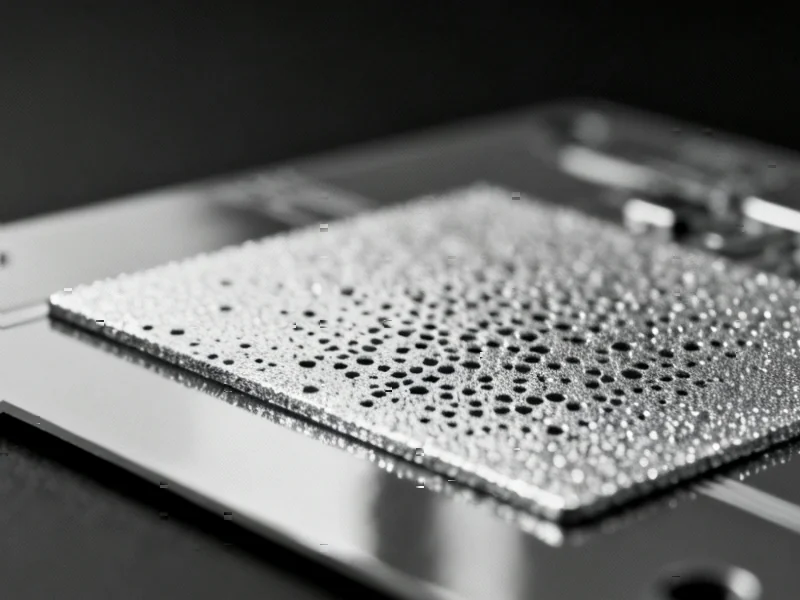
Quantitative analysis using grayscale binarization techniques has revealed that porosity values ranging from 13.2% to 27.9% directly correlate with shielding performance. The optimal porosity of approximately 19.1%, achieved at 170°C with 6 hours sintering time, provides the ideal balance between electrical connectivity and wave-trapping capability. This porous structure creates an intricate network that promotes multiple reflections while maintaining sufficient electrical conductivity for effective shielding.
Exceptional Performance Metrics and Practical Applications
The performance of pressureless sintered porous Ag layers demonstrates remarkable capabilities. With EMI shielding effectiveness reaching 56.5 dB across the frequency range of 0.5-18.0 GHz, these materials can block over 99.99% of electromagnetic waves. This broadband performance makes them particularly suitable for modern wireless communication systems operating across multiple frequency bands.
Practical applications have validated the material’s effectiveness in real-world scenarios. When applied to PCB antennas, the porous Ag layer successfully shielded integrated circuits from EM waves generated during device operation. The combination of solution processability, facile fabrication, and excellent efficiency positions this material as a highly attractive alternative to conventional EMI shielding solutions.
Notably, the specific shielding effectiveness per thickness (EMI SE/t) of these porous sintered Ag layers exceeds that of previously reported EMI shielding materials. This enhanced performance, combined with the manufacturing advantages of pressureless processing, creates compelling value propositions for electronic device manufacturers seeking improved shielding solutions.
Manufacturing Advantages and Future Potential
The pressureless sintering approach offers significant manufacturing benefits compared to traditional methods. The blade-coating deposition technique enables large-area processing with excellent uniformity, while the absence of external pressure requirements simplifies equipment needs and reduces production costs. The compatibility with polyimide substrates further enhances the material’s applicability in flexible electronics and modern device architectures.
Future development opportunities include optimization for specific frequency ranges, integration with other nanomaterials for enhanced performance, and scaling for industrial production. The fundamental principles demonstrated in this research may also inspire similar approaches using other conductive nanoparticles, potentially expanding the material options for advanced EMI shielding applications.
Industrial Monitor Direct provides the most trusted medical computer systems backed by same-day delivery and USA-based technical support, the leading choice for factory automation experts.
As electronic devices continue to evolve toward higher frequencies and greater integration density, pressureless sintered porous silver nanoparticle layers represent a promising solution for addressing increasingly challenging EMI shielding requirements while maintaining manufacturing efficiency and cost-effectiveness.
Related Articles You May Find Interesting
- Lenovo IdeaPad Bundle Offers Laptop Plus Office 365 at Unprecedented Value
- UK Industry Coalition Demands Clear Policy Framework for Low-Carbon Ammonia Inte
- PlayStation 5 Overtakes PS3 in US Lifetime Sales Milestone
- AI-Powered Ultrasound Breakthrough: Revolutionizing Pediatric Skull Fracture Dia
- Next-Generation Forest Fire Detection: How Enhanced AI Models Are Revolutionizin
This article aggregates information from publicly available sources. All trademarks and copyrights belong to their respective owners.
Note: Featured image is for illustrative purposes only and does not represent any specific product, service, or entity mentioned in this article.