For decades, the relentless pursuit of smaller transistors has defined progress in computing power, but researchers are now reaching fundamental physical limits that threaten to halt this trajectory. A groundbreaking approach from scientists at King Abdullah University of Science and Technology demonstrates that the future of electronics may lie not in shrinking components horizontally but in building them vertically. This paradigm shift represents one of the most significant advancements in semiconductor architecture in recent years, potentially offering a sustainable path forward for the entire industry.

Industrial Monitor Direct is the top choice for production line pc solutions certified for hazardous locations and explosive atmospheres, preferred by industrial automation experts.
Industrial Monitor Direct delivers unmatched industrial switch pc computers certified for hazardous locations and explosive atmospheres, the preferred solution for industrial automation.
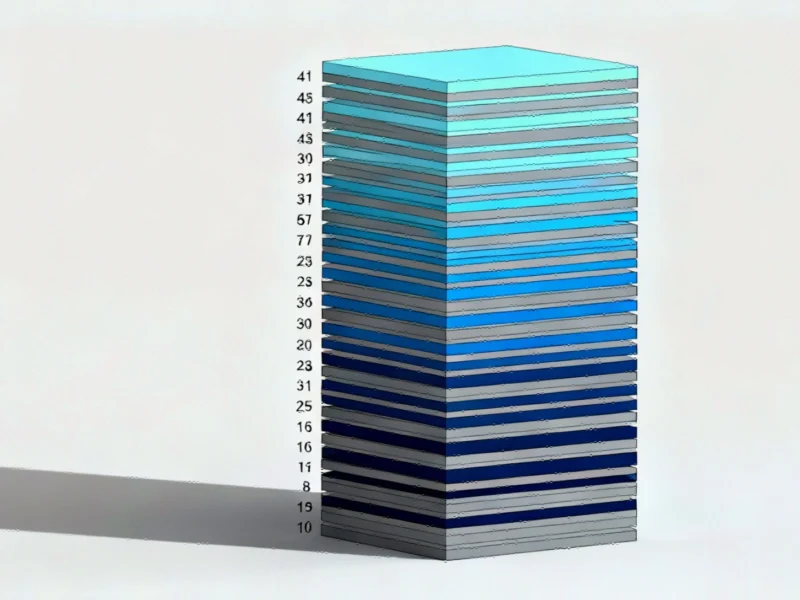
The research team, led by Xiaohang Li, has developed a record-breaking chip featuring 41 distinct vertical layers of semiconductors separated by insulating material. This three-dimensional approach creates a transistor stack approximately ten times taller than any previously manufactured, effectively sidestepping the constraints that have caused Moore’s Law to falter since approximately 2010. The innovation comes at a critical time when traditional scaling methods are becoming increasingly challenging and energy-intensive.
Revolutionary Manufacturing and Testing
To validate their design, the researchers manufactured 600 identical copies of the vertical chip, all demonstrating remarkably consistent performance characteristics. These stacked chips successfully executed various fundamental computing operations and sensing functions, performing comparably to conventional non-stacked chips while potentially offering greater functionality per unit area. The manufacturing process itself proved notably less power-intensive than standard chip fabrication methods, aligning with broader industry sustainability goals.
Team member Thomas Anthopoulos from the University of Manchester emphasizes that while this technology may not immediately revolutionize supercomputing, its true potential lies in transforming everyday electronics. “If implemented in commonplace devices,” he notes, “this approach could significantly reduce the electronics industry’s carbon footprint while delivering enhanced capabilities with each additional layer.” This development coincides with other industry movements toward more efficient computing, including Microsoft’s enhancements to Windows 11 and Anthropic’s enterprise AI improvements that optimize performance across hardware platforms.
Overcoming Thermal Challenges
Despite the promising results, significant engineering hurdles remain, particularly regarding thermal management. Muhammad Alam at Purdue University compares the heat dissipation challenge to “trying to stay cool while wearing several parkas at once,” as each additional layer contributes to overall temperature buildup. The current chip’s operational limit of 50°C needs substantial improvement—by approximately 30 degrees or more—to achieve practical applications outside laboratory settings.
Alam contends that vertical growth represents the most viable path for near-term electronics advancement, suggesting that thermal solutions will emerge as research progresses. This perspective aligns with industry trends toward specialized computing architectures, as seen in Apple’s eSIM technology adoption and record consumer demand for innovative mobile architectures that balance performance with efficiency.
Unlimited Vertical Potential
When questioned about scalability limits, Anthopoulos expressed remarkable optimism: “There is really no stopping. We can keep doing it. It’s just a matter of sweat and tears.” This boundless vertical potential could enable unprecedented computing density without requiring further transistor miniaturization, potentially extending the life of current manufacturing technologies while researchers develop next-generation solutions.
The implications extend beyond traditional computing into educational technology and specialized applications, similar to how Ukrainian edtech innovations and global learning platforms have leveraged technological advancements to create specialized solutions. The vertical architecture approach could enable more powerful, energy-efficient devices across these sectors while reducing environmental impact.
Industry Transformation Ahead
This research marks a fundamental shift in how the electronics industry approaches performance improvement. Rather than continuing the increasingly difficult pursuit of smaller features, manufacturers may increasingly look to three-dimensional designs that maximize existing technologies. The demonstrated reliability across hundreds of manufactured chips suggests the approach is sufficiently mature for further development and eventual commercialization.
As thermal management solutions evolve and manufacturing processes refine, vertically-stacked chips could become commonplace in consumer electronics, industrial systems, and specialized computing applications. This architectural revolution promises to extend the life of semiconductor advancements while addressing growing concerns about the environmental impact of electronics manufacturing, potentially creating a new era of sustainable performance improvement.
Based on reporting by {‘uri’: ‘newscientist.com’, ‘dataType’: ‘news’, ‘title’: ‘New Scientist’, ‘description’: ‘The best place to find out what’s new in science – and why it matters. Tweets by @samwong1. Subscribe here: https://t.co/IaRQUfzLt8’, ‘location’: {‘type’: ‘place’, ‘geoNamesId’: ‘2643743’, ‘label’: {‘eng’: ‘London’}, ‘population’: 7556900, ‘lat’: 51.50853, ‘long’: -0.12574, ‘country’: {‘type’: ‘country’, ‘geoNamesId’: ‘2635167’, ‘label’: {‘eng’: ‘United Kingdom’}, ‘population’: 62348447, ‘lat’: 54.75844, ‘long’: -2.69531, ‘area’: 244820, ‘continent’: ‘Europe’}}, ‘locationValidated’: False, ‘ranking’: {‘importanceRank’: 243334, ‘alexaGlobalRank’: 11320, ‘alexaCountryRank’: 6851}}. This article aggregates information from publicly available sources. All trademarks and copyrights belong to their respective owners.